PCB Layout Services
We can design the Printed Circuit Board (PCB) of your electronics products ranging from simple (two-layer) to complex (ten-layers and up) circuit boards. Our solutions include the design of rigid, flex or mix (rigid-flex) boards while also combining mixed type of circuits (Analog and Digital) on the same substrate.
Our engineers have many years of experience developing PCBs for all type of industries:
▀ Consumer Electronics
▀ Medical Products
▀ Aerospace devices
▀ Industrial Controls
▀ Telecommunications
▀ Automotive
These are the typical activities and deliverables we perform more frequently for our customers:
Board updates
Many customers come to us with ancient designs that were developed many years ago and sometimes poorly documented or not documented at all. We can look at those files, import old formats into our new ECAD (electronic CAD) and update your printed circuit board designs with new Gerber Files so you can submit them to manufacturing.
Schematic Updates
This involves reviewing initial BOM (Bill of Materials), new symbol creation, footprint creation and association, etc. Also, as part of our comprehensive solution we can analyze your current Bill of Materials to identify risk components that you could potentially run into during production due to obsolescence or hard-to-find status with vendors.
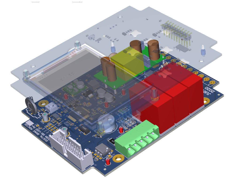
Interface with Mechanical design, creation of DXF files to determine board outline of the PCB. Today’s CAD software allow us to closely integrate the mechanical aspect of your product with the associated electronic board to review aspects like: Component location, heat dissipation, final assembly process, component-to-case clearance, connector locations, etc.
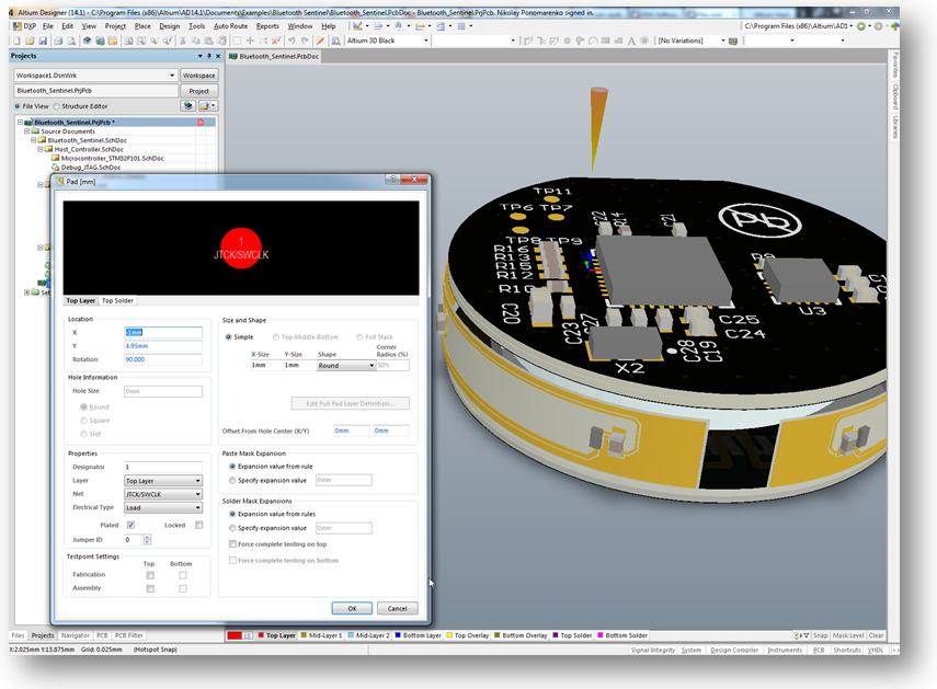
Component footprint creation and 3D model
This is needed so the board can be rendered as a 3D model in any CAD software. The subassembly model can be exportable to Solidworks as STEP format for mechanical review before sending PCB CAD/CAM files to manufacturing.
Layer Stackup
This is determining the right number copper layers your board should have, and its distribution in regards to the signals. The right choice will control the relationship cost vs performance of your PCB.
Placement and Routing of the electronic components.
PCB layout review to find last-minute pitfalls in the design.
Gerber File creation and documentation : Fabrication (FAB), Assembly (ASSY) and Drill (DRL) drawings.
Production support
Assisting customers with the interface with the PCB house. Do not worry about the “PCB Lingo” when you communicate with the manufacturing facility, we can handle that for you!
Test Fixture development
We can help your Company by automating the test process for the PCBAs using Automatic Functional Test performed on your newly assembled PCBAs.

