Uncategorized
Category Archives:Uncategorized
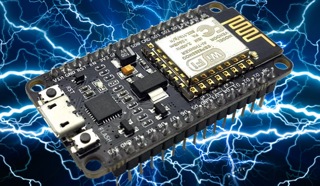
Measuring power consumption on ESP32 Modules
When using the ESP32 Module in applications that involve Wi-Fi access and battery-operated products, it is extremely important to properly qualify the power consumption of the ESP32 Module in the several power modes. The two most important reasons are:
- Designing the proper power supply or voltage regulator that powers the module
- Determine the right capacity value of the battery (for a battery operated device)
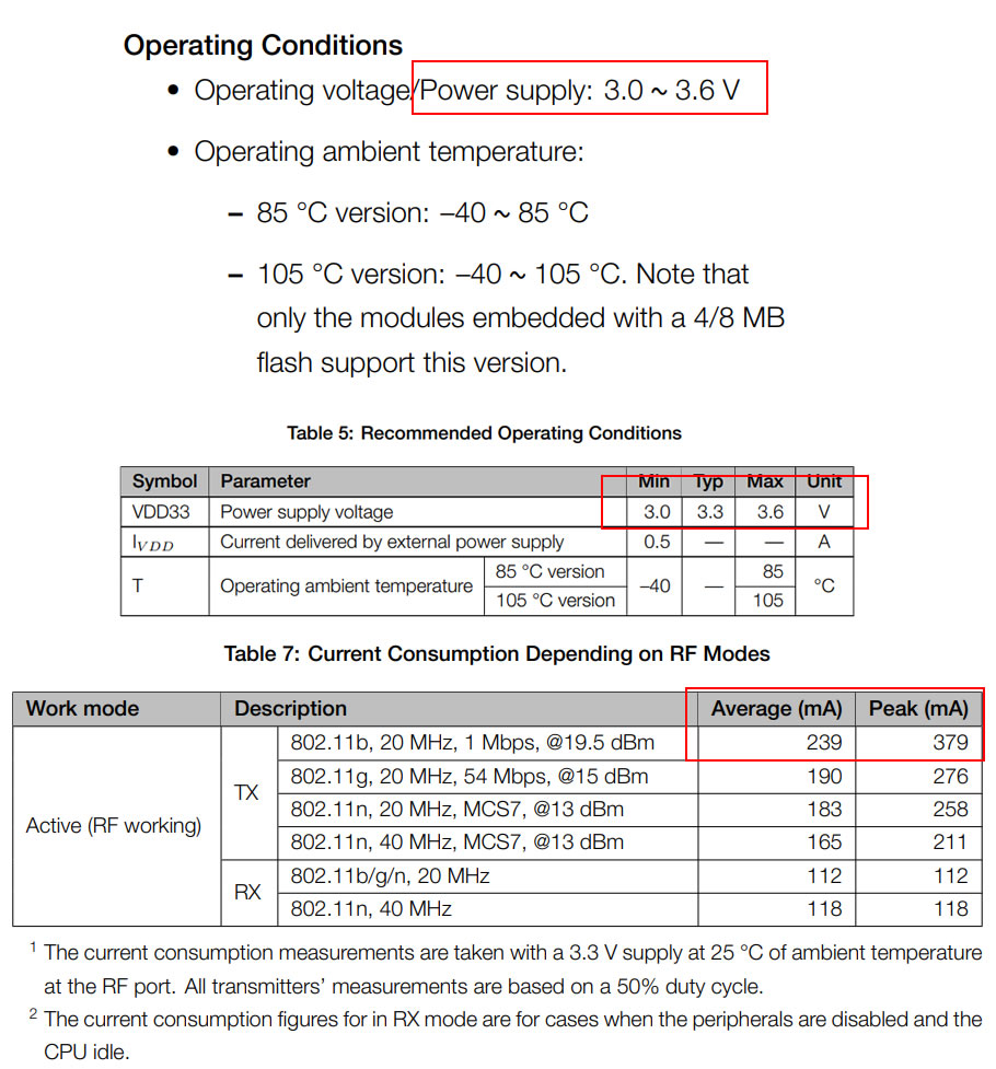
Let us check the datasheet of the ESP32WROOM32E module to get a baseline for our measurements:
In this opportunity we will measure the (current draw of the module in the following modes:
- Transmitting Mode. Wi-Fi, sending test packages (ping) to a remote server via Wi-Fi router.
- Sleep Mode
/*
This example code is in the Public Domain (or CC0 licensed, at your option.)
Unless required by applicable law or agreed to in writing, this
software is distributed on an "AS IS" BASIS, WITHOUT WARRANTIES OR
CONDITIONS OF ANY KIND, either express or implied.
*/
#include <string.h>
#include "freertos/FreeRTOS.h"
#include "esp_wifi.h"
#include "esp_log.h"
#include "tcpip_adapter_types.h"
#include "lwip/err.h"
#include "lwip/sockets.h"
#include "lwip/sys.h"
#include "lwip/netdb.h"
#include "lwip/dns.h"
#include "ping/ping_sock.h"
static const char *TAG = "PING";
void cmd_ping_on_ping_success(esp_ping_handle_t hdl, void *args)
{
uint8_t ttl;
uint16_t seqno;
uint32_t elapsed_time, recv_len;
ip_addr_t target_addr;
esp_ping_get_profile(hdl, ESP_PING_PROF_SEQNO, &seqno, sizeof(seqno));
esp_ping_get_profile(hdl, ESP_PING_PROF_TTL, &ttl, sizeof(ttl));
esp_ping_get_profile(hdl, ESP_PING_PROF_IPADDR, &target_addr, sizeof(target_addr));
esp_ping_get_profile(hdl, ESP_PING_PROF_SIZE, &recv_len, sizeof(recv_len));
esp_ping_get_profile(hdl, ESP_PING_PROF_TIMEGAP, &elapsed_time, sizeof(elapsed_time));
#if 1
ESP_LOGI(TAG, "%d bytes from %s icmp_seq=%d ttl=%d time=%d ms",
recv_len, inet_ntoa(target_addr.u_addr.ip4), seqno, ttl, elapsed_time);
#else
wifi_ap_record_t wifidata;
esp_wifi_sta_get_ap_info(&wifidata);
ESP_LOGI(TAG, "%d bytes from %s icmp_seq=%d ttl=%d time=%d ms RSSI=%d",
recv_len, inet_ntoa(target_addr.u_addr.ip4), seqno, ttl, elapsed_time, wifidata.rssi);
#endif
}
void cmd_ping_on_ping_timeout(esp_ping_handle_t hdl, void *args)
{
uint16_t seqno;
ip_addr_t target_addr;
esp_ping_get_profile(hdl, ESP_PING_PROF_SEQNO, &seqno, sizeof(seqno));
esp_ping_get_profile(hdl, ESP_PING_PROF_IPADDR, &target_addr, sizeof(target_addr));
ESP_LOGW(TAG, "From %s icmp_seq=%d timeout", inet_ntoa(target_addr.u_addr.ip4), seqno);
}
void cmd_ping_on_ping_end(esp_ping_handle_t hdl, void *args)
{
ip_addr_t target_addr;
uint32_t transmitted;
uint32_t received;
uint32_t total_time_ms;
esp_ping_get_profile(hdl, ESP_PING_PROF_REQUEST, &transmitted, sizeof(transmitted));
esp_ping_get_profile(hdl, ESP_PING_PROF_REPLY, &received, sizeof(received));
esp_ping_get_profile(hdl, ESP_PING_PROF_IPADDR, &target_addr, sizeof(target_addr));
esp_ping_get_profile(hdl, ESP_PING_PROF_DURATION, &total_time_ms, sizeof(total_time_ms));
uint32_t loss = (uint32_t)((1 - ((float)received) / transmitted) * 100);
if (IP_IS_V4(&target_addr)) {
ESP_LOGI(TAG, "\n--- %s ping statistics ---", inet_ntoa(*ip_2_ip4(&target_addr)));
} else {
ESP_LOGI(TAG, "\n--- %s ping statistics ---", inet6_ntoa(*ip_2_ip6(&target_addr)));
}
ESP_LOGI(TAG, "%d packets transmitted, %d received, %d%% packet loss, time %dms",
transmitted, received, loss, total_time_ms);
// delete the ping sessions, so that we clean up all resources and can create a new ping session
// we don't have to call delete function in the callback, instead we can call delete function from other tasks
esp_ping_delete_session(hdl);
}
/*
ping to targer forever
interval_ms:ping interval mSec. Default is 1000mSec.
task_prio:ping task priority. Default is 2.
target_host:target host url. if null,target is own gateway.
*/
esp_err_t initialize_ping(uint32_t interval_ms, uint32_t task_prio, char * target_host)
{
esp_ping_config_t ping_config = ESP_PING_DEFAULT_CONFIG();
if (strlen(target_host) > 0) {
/* convert URL to IP address */
ip_addr_t target_addr;
memset(&target_addr, 0, sizeof(target_addr));
struct addrinfo hint;
memset(&hint, 0, sizeof(hint));
struct addrinfo *res = NULL;
//int err = getaddrinfo("www.espressif.com", NULL, &hint, &res);
int err = getaddrinfo(target_host, NULL, &hint, &res);
if(err != 0 || res == NULL) {
ESP_LOGE(TAG, "DNS lookup failed err=%d res=%p", err, res);
return ESP_FAIL;
} else {
ESP_LOGI(TAG, "DNS lookup success");
}
if (res->ai_family == AF_INET) {
struct in_addr addr4 = ((struct sockaddr_in *) (res->ai_addr))->sin_addr;
inet_addr_to_ip4addr(ip_2_ip4(&target_addr), &addr4);
} else {
struct in6_addr addr6 = ((struct sockaddr_in6 *) (res->ai_addr))->sin6_addr;
inet6_addr_to_ip6addr(ip_2_ip6(&target_addr), &addr6);
}
freeaddrinfo(res);
ESP_LOGI(TAG, "target_addr.type=%d", target_addr.type);
ESP_LOGI(TAG, "target_addr=%s", ip4addr_ntoa(&(target_addr.u_addr.ip4)));
ping_config.target_addr = target_addr; // target IP address
} else {
// ping target is my gateway
tcpip_adapter_ip_info_t ip_info;
ESP_ERROR_CHECK(tcpip_adapter_get_ip_info(TCPIP_ADAPTER_IF_STA, &ip_info));
ESP_LOGI(TAG, "IP Address: %s", ip4addr_ntoa(&ip_info.ip));
ESP_LOGI(TAG, "Subnet mask: %s", ip4addr_ntoa(&ip_info.netmask));
ESP_LOGI(TAG, "Gateway: %s", ip4addr_ntoa(&ip_info.gw));
ip_addr_t gateway_addr;
gateway_addr.type = 0;
gateway_addr.u_addr.ip4 = ip_info.gw;
ESP_LOGI(TAG, "gateway_addr.type=%d", gateway_addr.type);
ESP_LOGI(TAG, "gateway_addr=%s", ip4addr_ntoa(&(gateway_addr.u_addr.ip4)));
ping_config.target_addr = gateway_addr; // gateway IP address
}
ping_config.count = ESP_PING_COUNT_INFINITE; // ping in infinite mode, esp_ping_stop can stop it
ping_config.interval_ms = interval_ms;
ping_config.task_prio = task_prio;
/* set callback functions */
esp_ping_callbacks_t cbs = {
.on_ping_success = cmd_ping_on_ping_success,
.on_ping_timeout = cmd_ping_on_ping_timeout,
.on_ping_end = cmd_ping_on_ping_end,
.cb_args = NULL
};
esp_ping_handle_t ping;
esp_ping_new_session(&ping_config, &cbs, &ping);
esp_ping_start(ping);
ESP_LOGI(TAG, "ping start");
return ESP_OK;
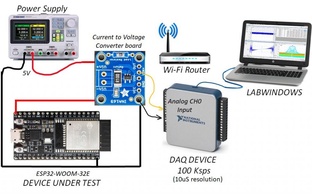
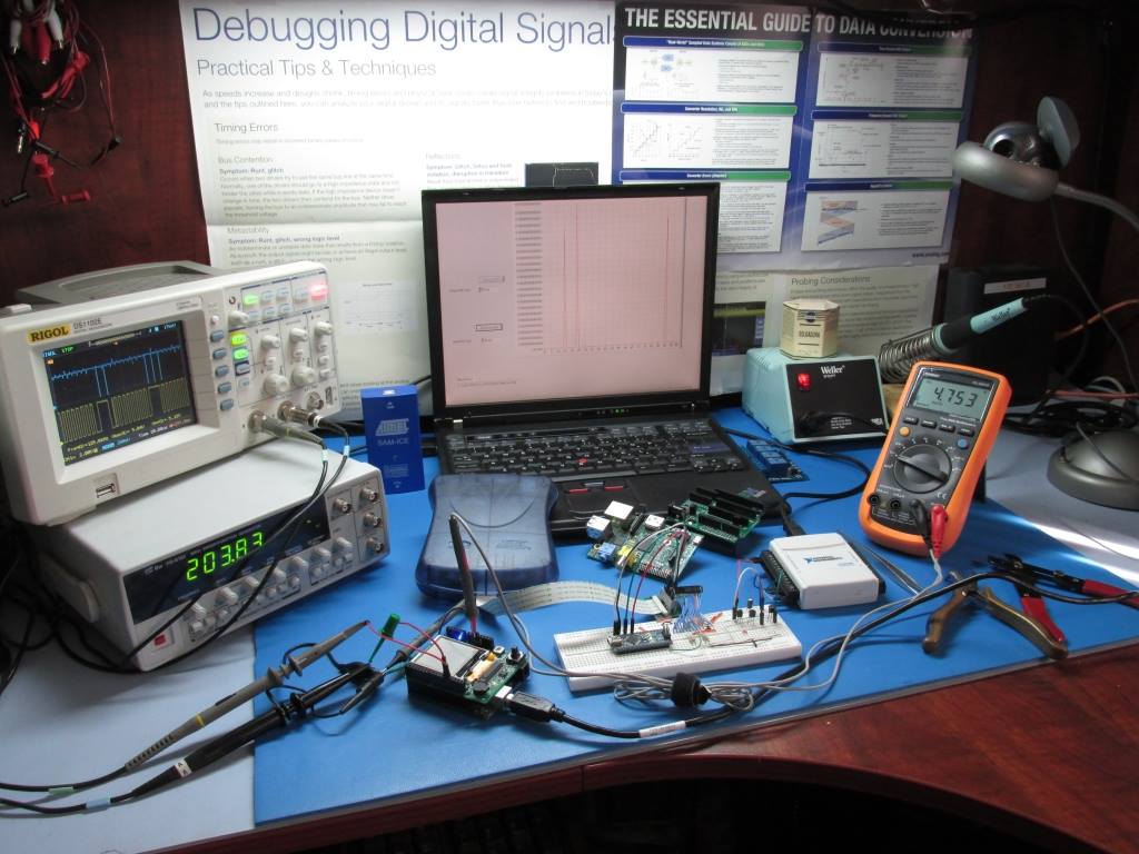
}Test Setup #1
Test Setup #2
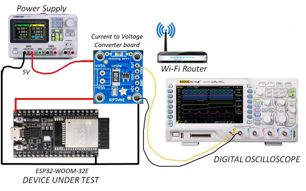
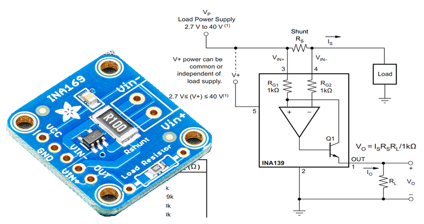
Current to Voltage converter board based on the INA169 chip
Using a sense resistor of 0.1 Ohms and a load resistor of 10K, the out voltage vs input current of the sensor board is calculated as this: Vo = Is Rs RL/1k, Vo= Is x 0.1 x 10K/1K Vo = Is; thus the ratio between input current and output voltage is 1.
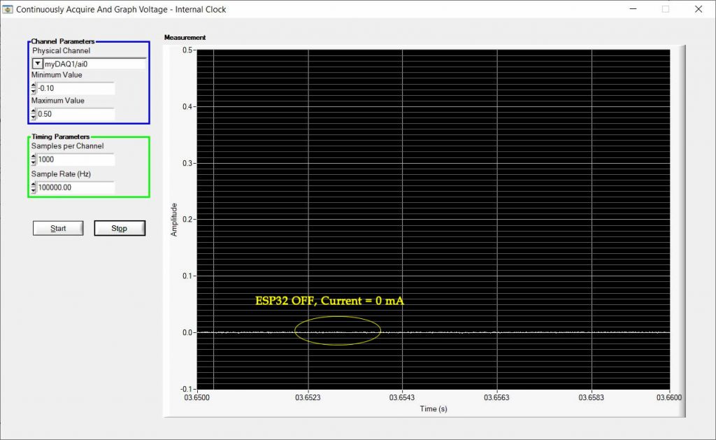
Results with DAQ Device:
With Module powered OFF
With Module transmitting Wi-Fi packages, measurement using the DAQ system
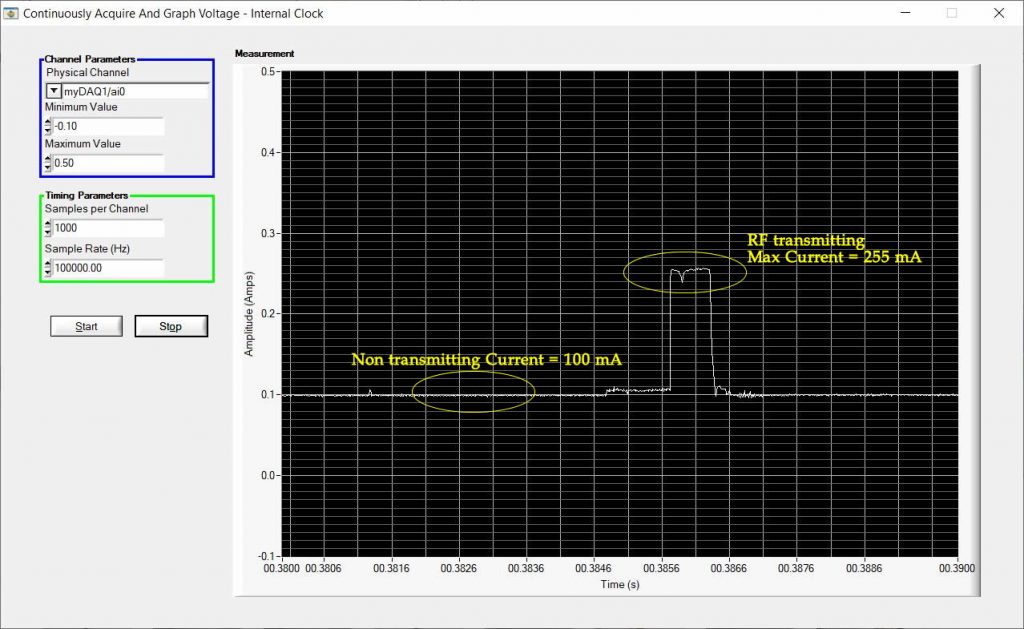
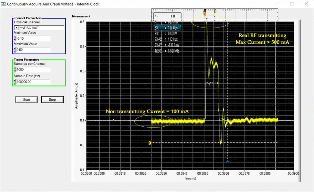
Here we discovered that average current of the ESP32 while transmitting Wi-Fi packets is 255mA, slightly higher than what is presented in the datasheet (239mA). Data captured does not show any significant peak of current. The current when not transmitting is about 100mA and that is what a normal multimeter should measure. The measurements with the DAQ device are nice, however, we have to take into account the limitations of this measurement due to the fact of the sampling rate of the DAQ, because of the limited samples acquired at high frequency, we may be losing peaks of current that occur faster than our sampling rate. Keep in mind these data when choosing a voltage regulator to power the ESP32 module, if the device is being powered by a typical USB port from a computer, which simultaneously is powering other devices you might encounter transmissions disruptions if the 500mA current limitation of the USB2.0 bus is surpassed.
Measurement using Test setup #2
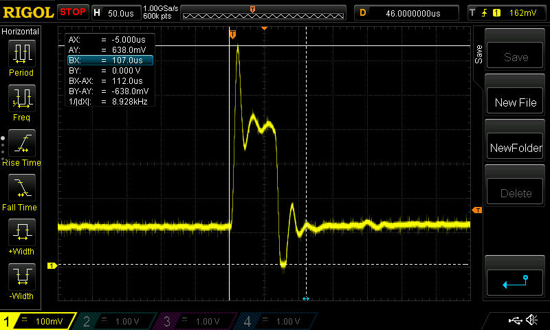
With the oscilloscope we have the advantage of high bandwidth for the measurement. We feed the output of the current sensor into CH1 of the oscilloscope and triggered the instrument with the same channel on the rising edge of the waveform. We discovered how the current peaks up to 638mA for about 25uS, and average current for transmissions is 400mA. The current consumption during no transmissions is still the same, 100mA. Total burst of current during transmissions last for 107uS.
Over imposing both measurements:
Note: All current measurements were taken while powering the ESP32 device at 3.3V. The datasheet of the module can be downloaded here:
esp32-wroom-32e_esp32-wroom-32ue_datasheet_en.pdf
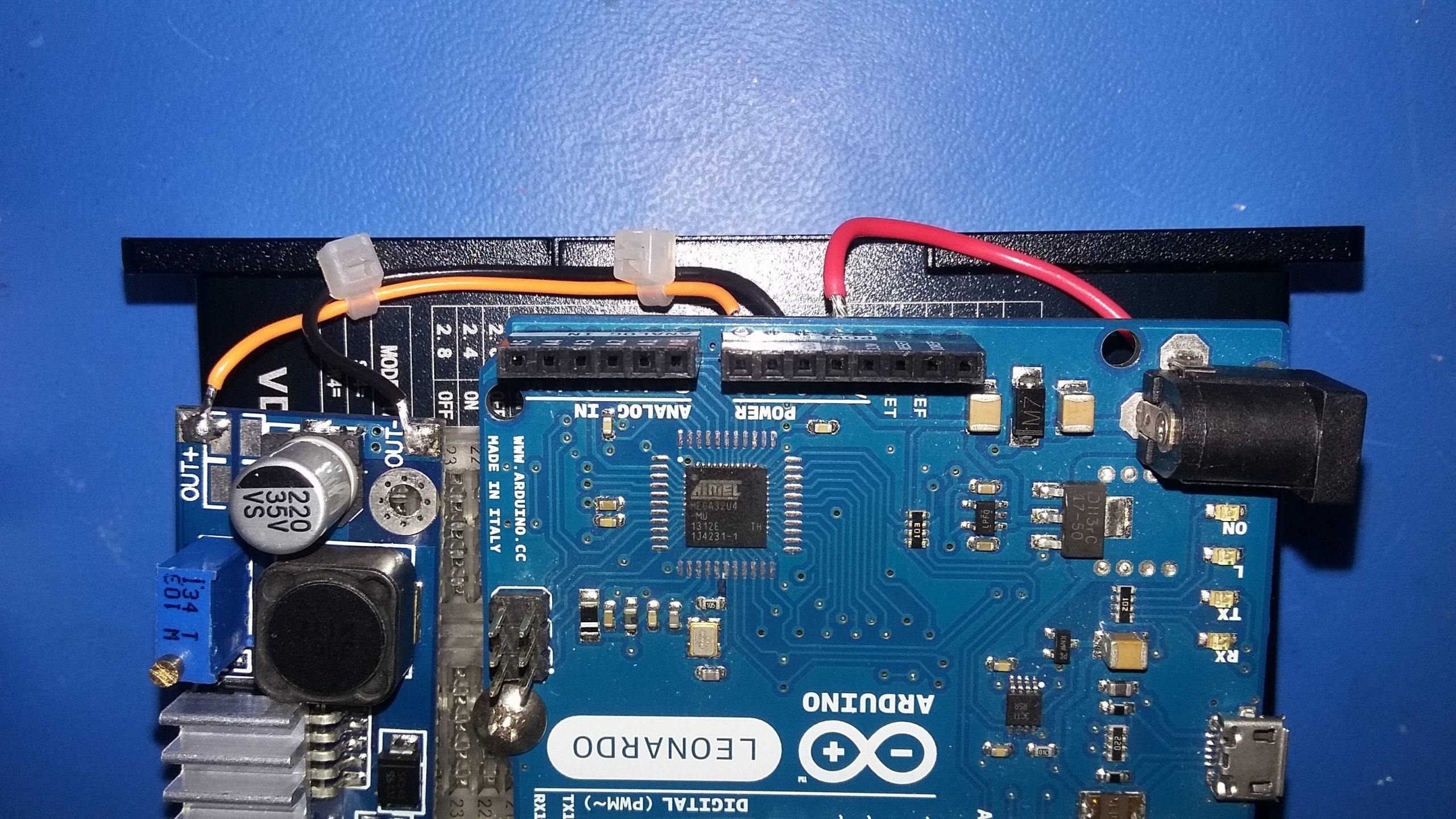
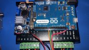
Controlling a high torque stepper Motor with Arduino
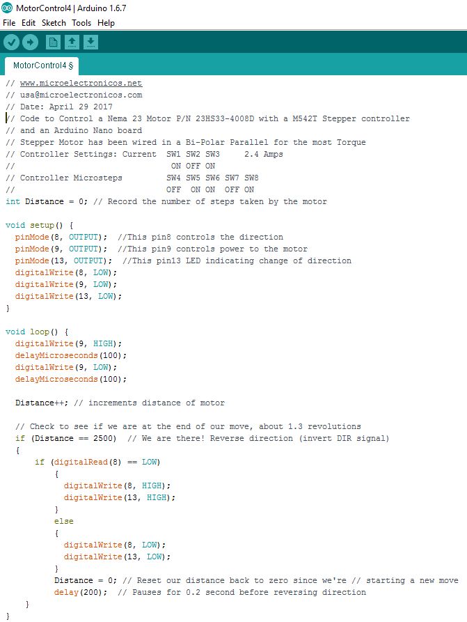
Check out our most recent project: Controlling a Stepper Motor (Nema23) and a Motor Driver M542T with Arduino. The motor driver uses a +24VDC power supply (2.5A) to provide high torque and speed to the stepper. The Arduino generates the control signals to control the driver (M542T). Basically two signals are being driven on the MT542T: Direction (DIR) and Speed (PUL). The PUL signal is PWM with the duty cycle depends on the current required by the motor. For this application the frequency of the PWM was chosen to be 5KHz (T= 200 uSec).


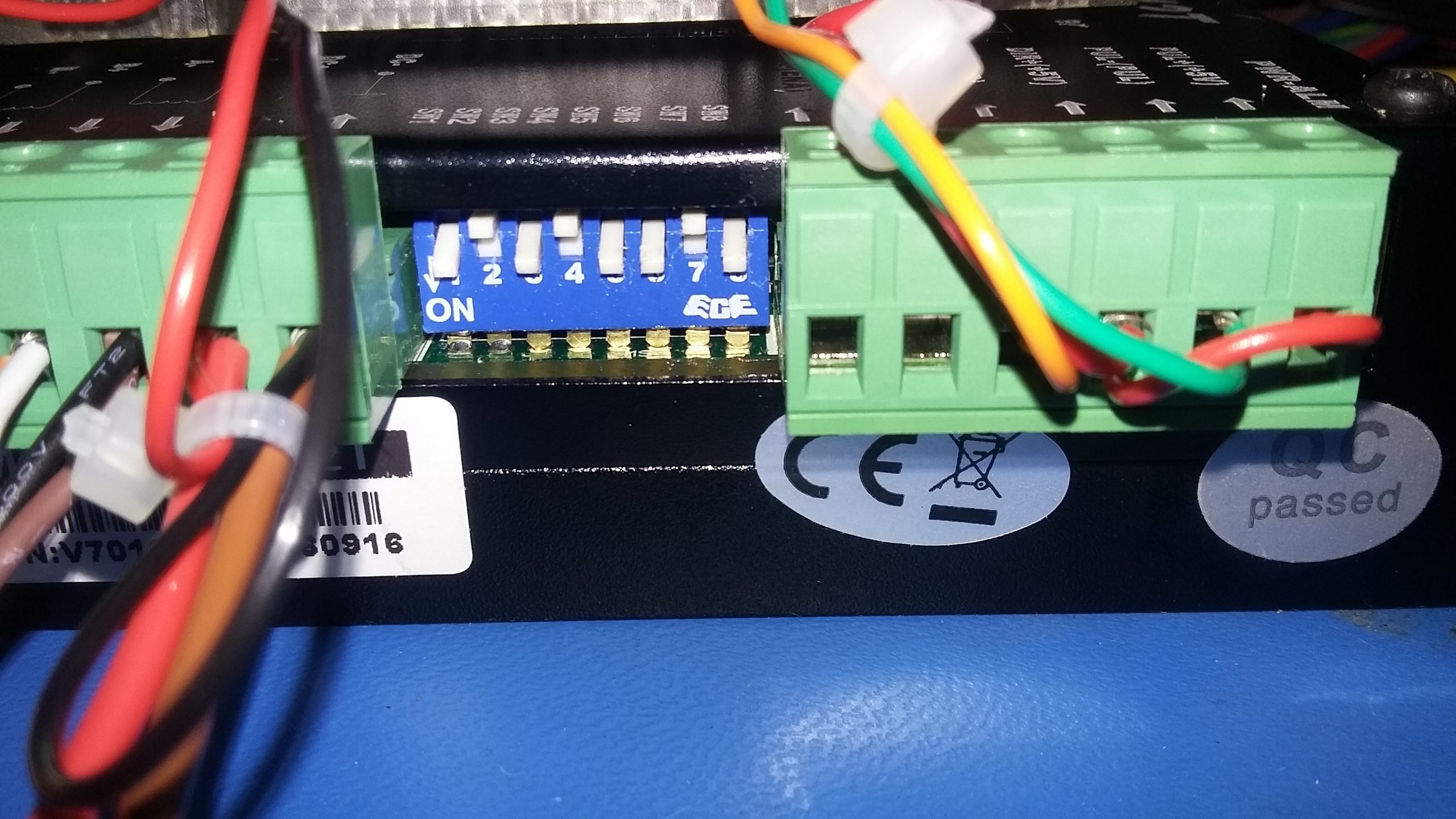
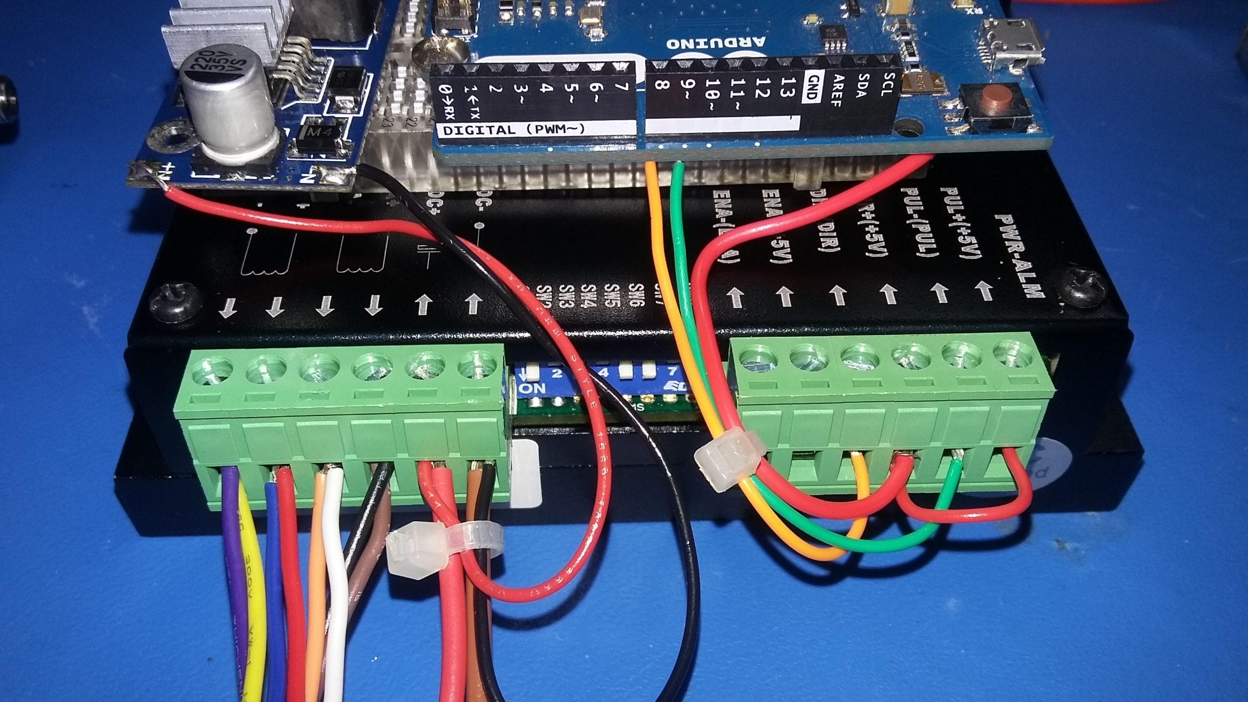
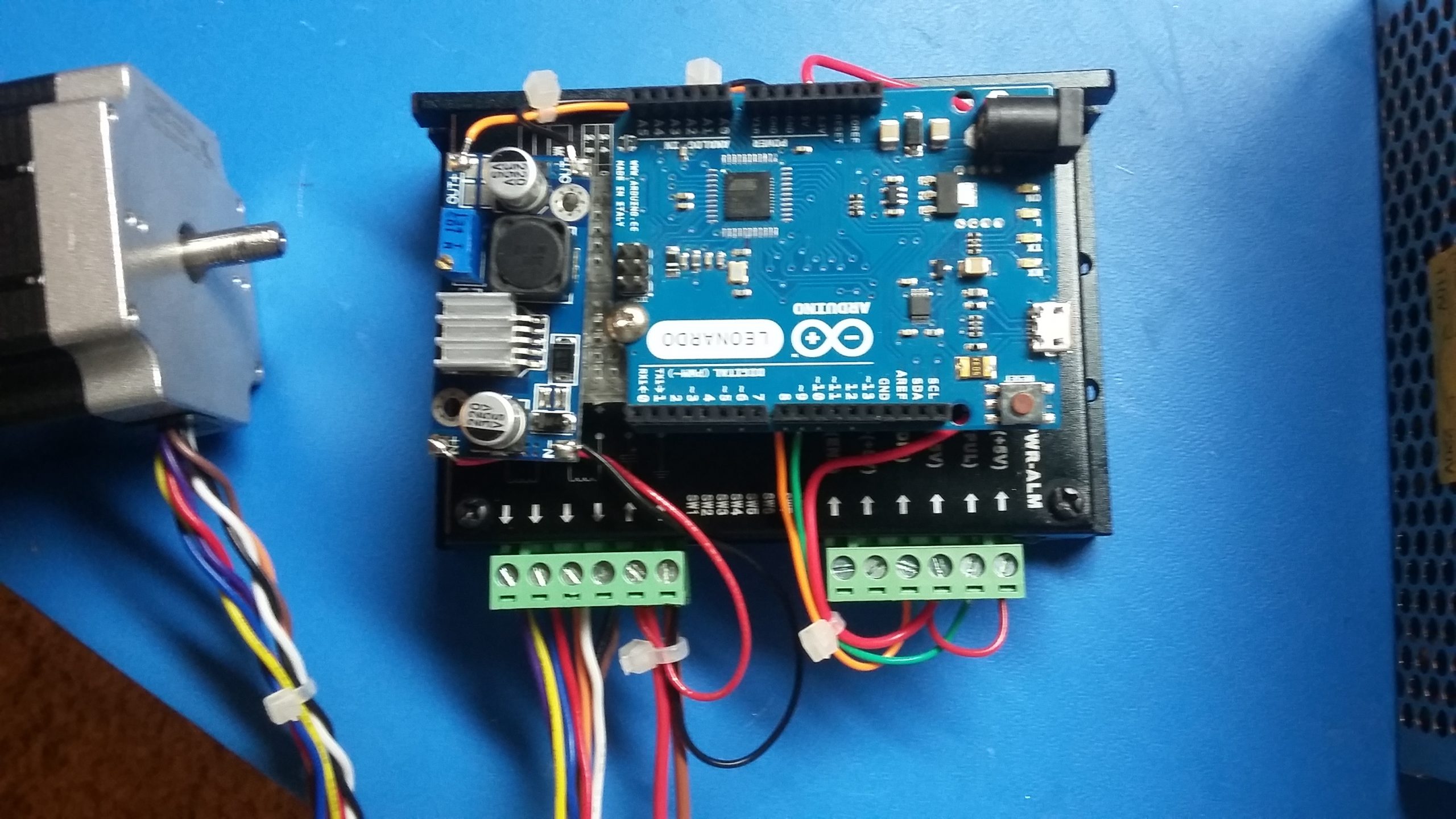
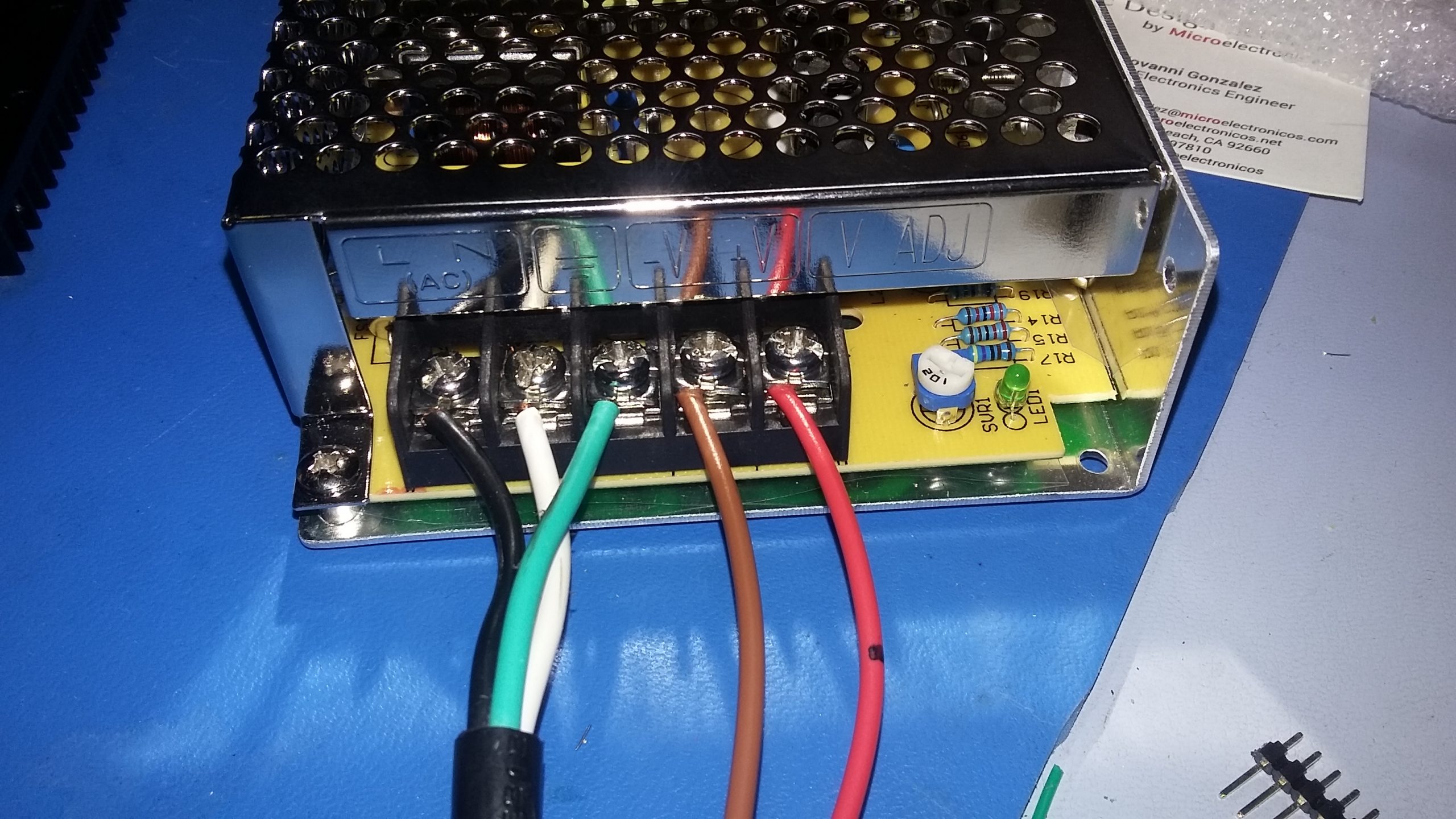
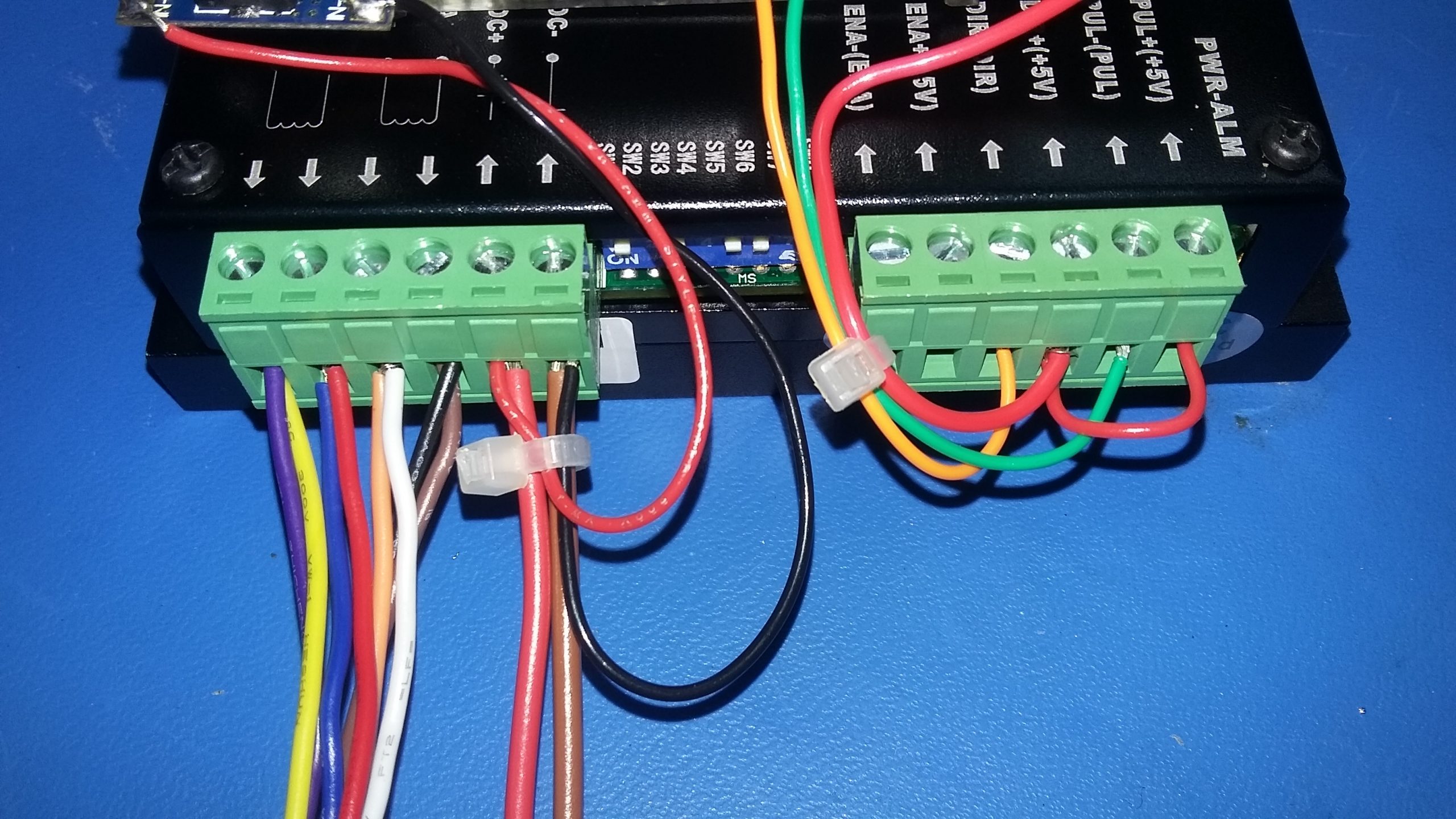
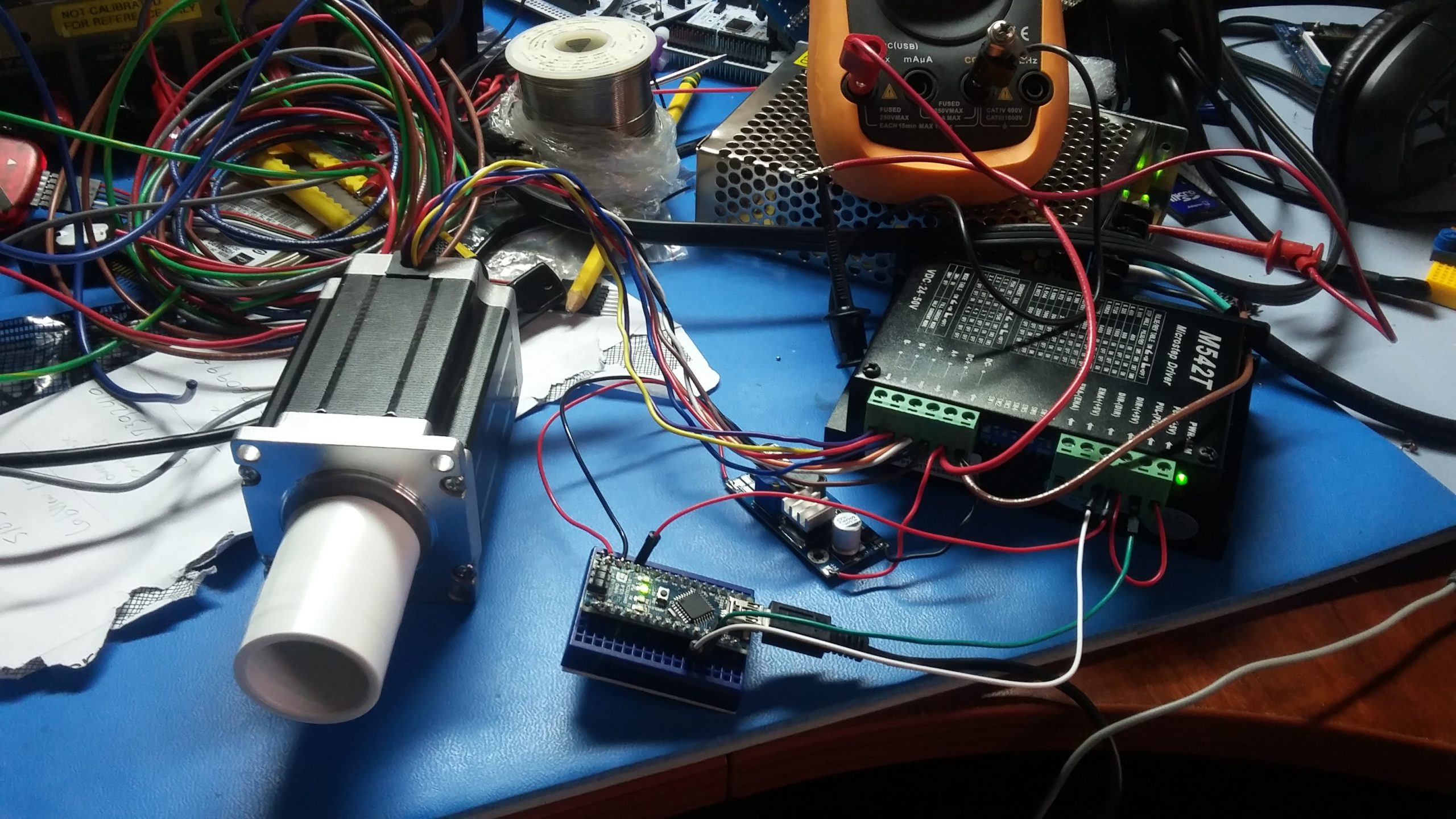
The electrical schematic we used is the following (see diagram below). You can use a different power supply (more current capability) if you require more torque in your application. In our case, the motor windings have been wired in a bipolar parallel configuration which provides a high torque at high speeds since it presents the lowest inductance (and resistance to the current). With this configuration the motor can provide up to 2.83N.m/400 oz-in (25 Lb per inch) and each phase can draw up to 5.66 A.
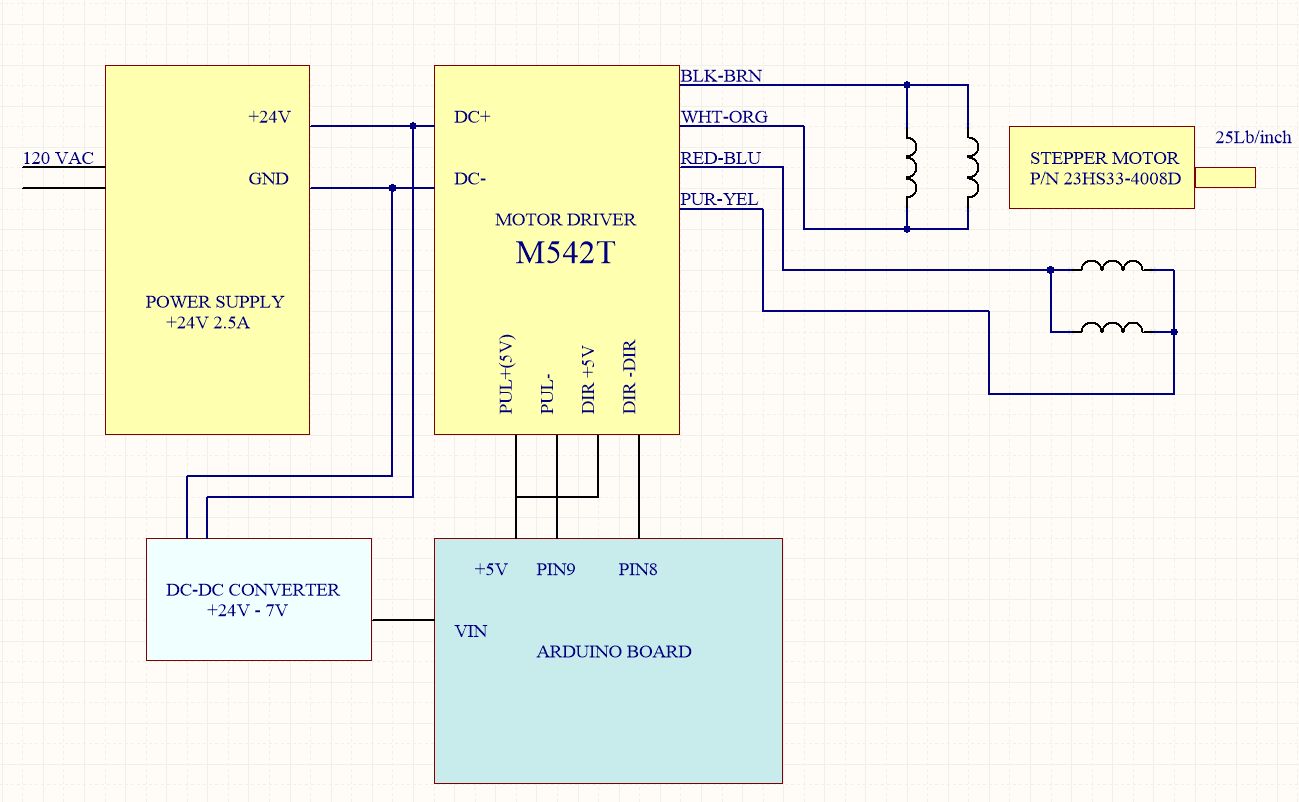
You can see the Arduino code below (any Arduino board can be used: Uno/Leonardo/Nano/Mega/Mini, or similar)
11 Myths About PCB Layout
Printed circuit boards (PCBs) have been an integral part of electronics for many years. Through the years, electronic devices are getting smaller and more complex and so are the PCBs needed to connect the components in an efficient manner. As robotics and electronic design begin to be taught as early as grade school, the art of PCB layout becomes more meaningful. What follows are 11 common myths about PCB layout:
1. Once an electrical schematic is complete, the hard work is over.
The layout of a PCB from an electrical schematic seems like a simple two-step process: Place the required components and connect the wires/traces to the appropriate point on the components. However, many factors still must be considered when getting from the schematic to a finished PCB design suitable for prototype or production. Some of these include physical design constraints (size and placement of the parts, orientation of parts on opposite side of PCB), electrical interaction between signals, heat dissipation, and signal loss through the wires/traces. All of these and more still require an engineering mind to accomplish a working design.
2. PCB layout for prototyping and production are similar.
Depending on the intent of your design, you may make vastly different choices in the types of components to be used. For a prototype or proof-of-concept design, you may opt for through-hole parts for as many parts as you can. They’re relatively inexpensive and easy to solder to your PCB.
However, in a production design, you want to shy away from use of through-hole parts in favor of surface-mount parts. Through-hole parts are costly to assemble in volume and can dramatically increase production cost due to increased board size, layer count, component availability delays, etc. Also, reducing the number of unique parts on the bill of materials (BOM) is another way to minimize production cost.
3. Components can be placed almost anywhere on the board, and it will result in an effective PCB.
Planning your PCB layout in terms of modules, similar to your schematic, is a much more effective way to layout your design. Components close in proximity in the schematic should also be in close proximity in the layout. Most designers like to think of the design in terms of modules. One common error in layout is to ignore the physical height of a component and its location with respect to case or neighboring boards.
4. Power distribution is not a critical element in layout.
Power delivery is critical in the performance of any circuit. Some parts require much more power, and better conditioned power, than others. This has to be taken into account early in the design or circuit performance will suffer.
Supplying power to all of the various components on a PCB can be done in several ways. But, regardless of the method, it needs to be planned so as to deliver the correct current to each component without creating voltage drops by unnecessarily running power in series, creating longer paths, or choking down the current with trace size or a chopped-up power plane (a plane with poorly placed through vias that will limit the current flow).
5. Standard DRC settings are applicable for all designs.
The best strategy to getting the PCB when you want and how you want, at a cost that doesn’t kill your project, is to know your PCB manufacturer and tailor your “in tool” design-rule-check (DRC) settings to their manufacturing “sweetspot, whenever possible.” Working with a trusted manufacturing partner (and to their strengths) maximizes the success rate of the PCB design. Just because you can design it, doesn’t mean every PCB manufacturer can build it.
Another tool that saves time and unnecessary cost to a project is a design-for-manufacturability (DFM) analysis on your completed design by the manufacturer, prior to manufacturing. If your PCB fabricator makes a suggestion for improvement, it may be worth the effort to alter your design slightly in order to produce a more reliable and cost-effective product. You might even want to stop your current production cycle and rework your design before continuing. While this sounds painful, receiving boards that fail in the field due to manufacturing defects caused by design flaws is even worse.
6. Any part published in a library is ready to place on a layout.
Not all parts libraries are created equal. Discrepancies often exist between the component footprints and the technical datasheet. Sometimes it’s a matter of the size, or pin assignments, or even the orientation. Everything may look okay at the layout stage, but when the physical part will not fit into the footprint, delays and spin revisions can ensue. Take the extra time to verify that the part matches the datasheet. Remember, it only takes one bad part to destroy a project.
7. Grouping of similar parts in a design is a good use of space.
It might seem like grouping similar parts of a PCB into a common area is the best use of space, but as we have discussed above, the parts should be located in relative proximity to its space in the schematic, limiting the distance that the signal must travel and eliminating unnecessary routing on the board. This is especially true for microcontrollers and their caps.
Minimizing the trace lengths from the controller to the cap decouples noise from the power supply to ground, creating a better result. Sometimes a schematic will have all of the decoupling capacitors grouped on one page, away from the component pins that they service. You will need to make that association and place those parts logically in order to ensure proper circuit function.
8. Auto-routing a layout, once components are placed, saves time and money.
While the intent of an auto-router is to do just that, the execution of the algorithm is not 100% foolproof. Oftentimes, the results of an entirely auto-routed board may connect all of the necessary points, but it can result in a poor design from electrical and manufacturability standpoints. Route the clocks, route the power/ground, route any critical nets; then, if you must, run the auto-router. Once the auto-route is complete, go back and see if you can clean up any poorly routed nets.
9. Minimum trace widths are adequate for all traces in a design.
High-speed lines sometimes have impedance requirements that will govern trace widths of these traces. Make sure that these requirements are taken into account when routing them. Also, the current load of a power net should be considered before routing. Traces with a high current load need to be sized large enough to carry that current without overheating. Use of a trace width calculator, readily available on the internet, can simplify this calculation significantly.
10. My design passed all of the DRC checks in my tool; therefore, it should work as I expect.
Even powerful DRC tools have limitations as to the extent of the design rules. They simply cannot replace good engineering practices. An example is the return paths to ground. The DRC can verify that they exist, but not necessarily determine the size, path length, and trace geometry to get the best electrical results.
11. Now that my design is finished, all I have left to do is export my Gerber files and order my PCBs.
Unfortunately, there are pitfalls in the Gerber extraction process of most tools, potentially resulting in the PCB manufacturer seeing one thing and you seeing another in the design tool. Verify your output (Gerber) files before submitting them to be built.
As the need increases for engineers, inventors and hobbyists to include a PCB in their projects, so does the need for knowledge transfer for PCB layout. Awareness of the myths of layout and adjusting accordingly can improve the time to market and cost of the project simply by reducing design spins and additional troubleshooting and engineering evaluations.
Author: Mathew Stevenson, source: http://electronicdesign.com/boards/11-myths-about-pcb-layout

Make it Small, Make it Fast, Make it First: Miniaturizing IoT Designs
Summary
As we wirelessly connect more and more devices to the Internet, electronics engineers face several challenges, including packaging a radio transmitter into existing device real estate and the demand to build increasingly smaller devices. In this webinar, we’ll explore some of the obstacles that come with the size expectations of IoT designs, from concerns around antenna integration to new packaging options that can help solve issues like detuning and size limitations.
Join our hour-long webinar on January 11, 2017 at 10:00 AM and get your questions answered during our Live Q&A session at the end.

Is Tomorrow’s Embedded-Systems Programming Language Still C?
What is the best language in which to code your next project? If you are an embedded-system designer, that question has always been a bit silly. You will use, C—or if you are trying to impress management, C disguised as C++. Perhaps a few critical code fragments will be written in assembly language. But according to a recent study by the Barr Group, over 95 percent of embedded-system code today is written in C or C++.
TDK Swears by Sensor Fusion in $1.3 Billion Deal for InvenSense
Sensor fusion, a technology that merges data from multiple sensors to make unique conclusions, was the hidden gem in TDK’s recent acquisition of InvenSense, a maker of gyroscopes and other motion sensors.
TDK agreed last week to pay $1.3 billion for InvenSense, one of the largest makers of gyroscopes for measuring motion and rotation, sending a signal that it wants to prevent machines from ever losing their bearings. It plans to do so with technology that simulates how human senses work in tandem.
The acquisition is one of the smaller deals in a semiconductor industry that has consolidated around slowing sales and the rising cost of product development. But it also marks a big bet on sensor fusion, a technology that coordinates different sensors to compute something more than could be determined by a lone device.

CES 2017: What to expect at the massive Las Vegas tech show
CES 2017 promises to live up to the Las Vegas expo’s reputation as the place to see what’s next in tech. Whether eye-popping TVs, futuristic cars, shiny mobile devices, mind-boggling virtual reality or amazing cameras, CES rarely disappoints when it comes to showcasing unbelievable tech.
The official CES 2017 dates are January 5 through January 8, 2017, though as always, there will be plenty of pre-show announcements on January 3 and January 4.
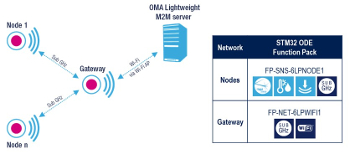
Build a 6LoWPAN wireless sensor network
The STM32 Open Development Environment provides developers with end-to-end solutions to explore and validate design concepts. Using a combination of ODE components, it’s now possible to build a wireless sensor network based on 6LoWPAN connectivity leveraging a wide range of sensor technologies and make sensor data accessible via the Internet for further use through a Wi-Fi bridge.
Welcome to Microelectronicos!
Microelectronicos is an electronics design consulting company, specialized in electronic circuit design, PCB layout, Embedded Software and mechanical/industrial design. Our seasoned and experienced designers can guide you through the engineering design process and make your idea a product reality.

Designing a USB battery charging device
Microelectronicos recently designed and prototype a USB-based battery charging device to allow mobile sensors to be charged from the computer in about 30 minutes. Using the latest technology in PMIC (Power Management Integrated Circuit) by Texas instruments we were able to design a very reliable product which is very cheap to manufacture and performs 100% with our customer specifications.
-
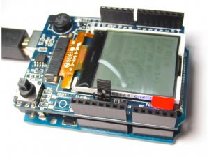 LCD Shield Monocromatic for Arduino
$80.00
LCD Shield Monocromatic for Arduino
$80.00
-
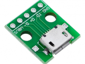 Adapter Micro USB
$45.00
Adapter Micro USB
$45.00