Monthly Archives: March 2017

11 Myths About PCB Layout
Printed circuit boards (PCBs) have been an integral part of electronics for many years. Through the years, electronic devices are getting smaller and more complex and so are the PCBs needed to connect the components in an efficient manner. As robotics and electronic design begin to be taught as early as grade school, the art of PCB layout becomes more meaningful. What follows are 11 common myths about PCB layout:
1. Once an electrical schematic is complete, the hard work is over.
The layout of a PCB from an electrical schematic seems like a simple two-step process: Place the required components and connect the wires/traces to the appropriate point on the components. However, many factors still must be considered when getting from the schematic to a finished PCB design suitable for prototype or production. Some of these include physical design constraints (size and placement of the parts, orientation of parts on opposite side of PCB), electrical interaction between signals, heat dissipation, and signal loss through the wires/traces. All of these and more still require an engineering mind to accomplish a working design.
2. PCB layout for prototyping and production are similar.
Depending on the intent of your design, you may make vastly different choices in the types of components to be used. For a prototype or proof-of-concept design, you may opt for through-hole parts for as many parts as you can. They’re relatively inexpensive and easy to solder to your PCB.
However, in a production design, you want to shy away from use of through-hole parts in favor of surface-mount parts. Through-hole parts are costly to assemble in volume and can dramatically increase production cost due to increased board size, layer count, component availability delays, etc. Also, reducing the number of unique parts on the bill of materials (BOM) is another way to minimize production cost.
3. Components can be placed almost anywhere on the board, and it will result in an effective PCB.
Planning your PCB layout in terms of modules, similar to your schematic, is a much more effective way to layout your design. Components close in proximity in the schematic should also be in close proximity in the layout. Most designers like to think of the design in terms of modules. One common error in layout is to ignore the physical height of a component and its location with respect to case or neighboring boards.
4. Power distribution is not a critical element in layout.
Power delivery is critical in the performance of any circuit. Some parts require much more power, and better conditioned power, than others. This has to be taken into account early in the design or circuit performance will suffer.
Supplying power to all of the various components on a PCB can be done in several ways. But, regardless of the method, it needs to be planned so as to deliver the correct current to each component without creating voltage drops by unnecessarily running power in series, creating longer paths, or choking down the current with trace size or a chopped-up power plane (a plane with poorly placed through vias that will limit the current flow).
5. Standard DRC settings are applicable for all designs.
The best strategy to getting the PCB when you want and how you want, at a cost that doesn’t kill your project, is to know your PCB manufacturer and tailor your “in tool” design-rule-check (DRC) settings to their manufacturing “sweetspot, whenever possible.” Working with a trusted manufacturing partner (and to their strengths) maximizes the success rate of the PCB design. Just because you can design it, doesn’t mean every PCB manufacturer can build it.

Another tool that saves time and unnecessary cost to a project is a design-for-manufacturability (DFM) analysis on your completed design by the manufacturer, prior to manufacturing. If your PCB fabricator makes a suggestion for improvement, it may be worth the effort to alter your design slightly in order to produce a more reliable and cost-effective product. You might even want to stop your current production cycle and rework your design before continuing. While this sounds painful, receiving boards that fail in the field due to manufacturing defects caused by design flaws is even worse.
6. Any part published in a library is ready to place on a layout.
Not all parts libraries are created equal. Discrepancies often exist between the component footprints and the technical datasheet. Sometimes it’s a matter of the size, or pin assignments, or even the orientation. Everything may look okay at the layout stage, but when the physical part will not fit into the footprint, delays and spin revisions can ensue. Take the extra time to verify that the part matches the datasheet. Remember, it only takes one bad part to destroy a project.
7. Grouping of similar parts in a design is a good use of space.
It might seem like grouping similar parts of a PCB into a common area is the best use of space, but as we have discussed above, the parts should be located in relative proximity to its space in the schematic, limiting the distance that the signal must travel and eliminating unnecessary routing on the board. This is especially true for microcontrollers and their caps.
Minimizing the trace lengths from the controller to the cap decouples noise from the power supply to ground, creating a better result. Sometimes a schematic will have all of the decoupling capacitors grouped on one page, away from the component pins that they service. You will need to make that association and place those parts logically in order to ensure proper circuit function.
8. Auto-routing a layout, once components are placed, saves time and money.
While the intent of an auto-router is to do just that, the execution of the algorithm is not 100% foolproof. Oftentimes, the results of an entirely auto-routed board may connect all of the necessary points, but it can result in a poor design from electrical and manufacturability standpoints. Route the clocks, route the power/ground, route any critical nets; then, if you must, run the auto-router. Once the auto-route is complete, go back and see if you can clean up any poorly routed nets.
9. Minimum trace widths are adequate for all traces in a design.
High-speed lines sometimes have impedance requirements that will govern trace widths of these traces. Make sure that these requirements are taken into account when routing them. Also, the current load of a power net should be considered before routing. Traces with a high current load need to be sized large enough to carry that current without overheating. Use of a trace width calculator, readily available on the internet, can simplify this calculation significantly.
10. My design passed all of the DRC checks in my tool; therefore, it should work as I expect.
Even powerful DRC tools have limitations as to the extent of the design rules. They simply cannot replace good engineering practices. An example is the return paths to ground. The DRC can verify that they exist, but not necessarily determine the size, path length, and trace geometry to get the best electrical results.

11. Now that my design is finished, all I have left to do is export my Gerber files and order my PCBs.
Unfortunately, there are pitfalls in the Gerber extraction process of most tools, potentially resulting in the PCB manufacturer seeing one thing and you seeing another in the design tool. Verify your output (Gerber) files before submitting them to be built.
As the need increases for engineers, inventors and hobbyists to include a PCB in their projects, so does the need for knowledge transfer for PCB layout. Awareness of the myths of layout and adjusting accordingly can improve the time to market and cost of the project simply by reducing design spins and additional troubleshooting and engineering evaluations.
Author: Mathew Stevenson, source: http://electronicdesign.com/boards/11-myths-about-pcb-layout
-
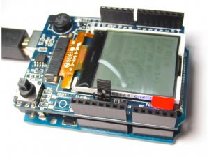 LCD Shield Monocromatic for Arduino
$80.00
LCD Shield Monocromatic for Arduino
$80.00
-
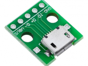 Adapter Micro USB
$45.00
Adapter Micro USB
$45.00